-
关注商城

关注官方微信
关注官方微信

销售咨询
技术支持

联系客服


 购前提示 |
常用产品货期为1-2天,非常用产品为一周; 进口产品、贵金属产品、订制规格产品,价格、货期影响因素较多。 关于货期、价格、质量规格等问题采购前,请于客服沟通。 |
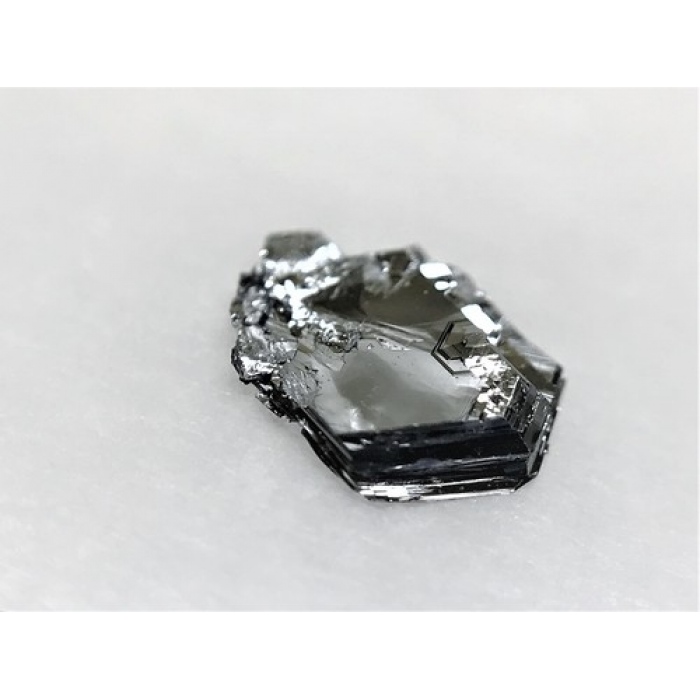
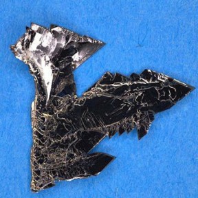
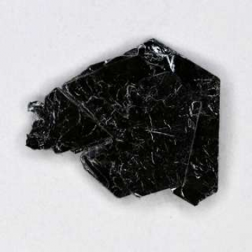
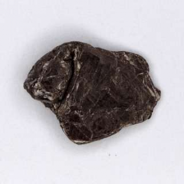
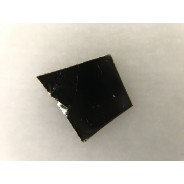
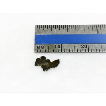
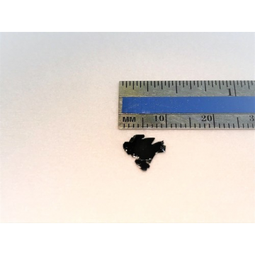
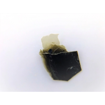
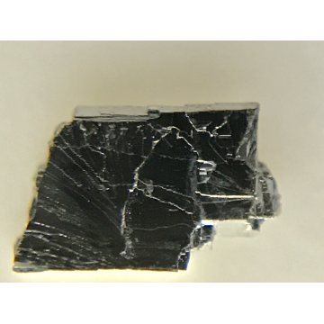
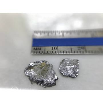
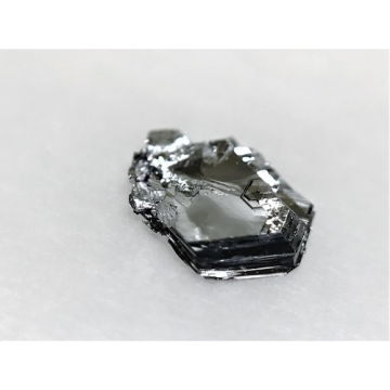
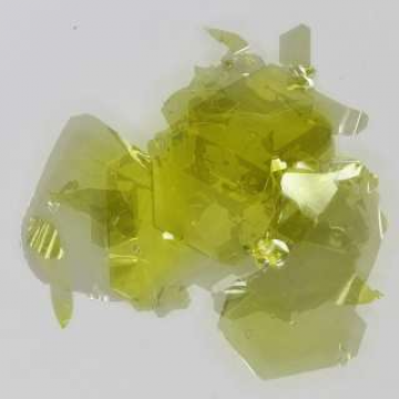
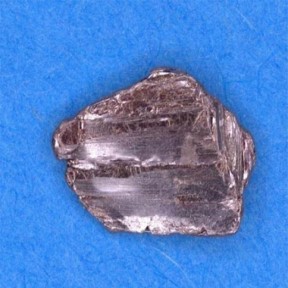
More than a decade of growth optimization in chemical vapor transport (CVT) as well as flux growth lead to our flawless MoS2 crystals. Our p-type MoS2 crystals are doped with Nb atoms at 1E17-5E18cm-3 range. These electronically doped vdW MoS2 crystals are treated as gold standards in 2D materials field. MoS2 crystals from 2Dsemiconductors are known for its superior valleytronic performance, perfect crystallization, defect free structure, extremely narrow PL bandwidths, clean PL spectra (free of bound exciton shoulders), and high carrier mobility. Thousands of scientific articles have cited us and used these crystals for scientific accuracy and clean signals. Please also see our n- and p-type MoS2 crystals doped with Au, Re, Nb, or other transition metal atoms.
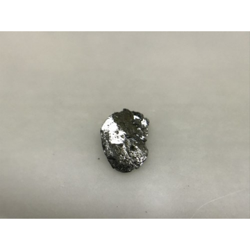
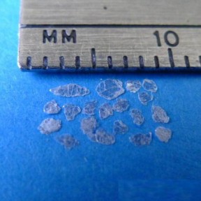
Please note that doping into TMDCs greatly reduce the crystallization time (growth speeds), thus electronically doped TMDCs measure smaller than undoped (intrinsic) TMDCs.
List of publications out of this product listed below this page.
Our company essentially provides doping for almost any layered materials including MoS2 crystals. P-type MoS2 samples are doped by Nb atoms at ~2E17cm-3 levels. Crystallinity, electronic, and optical quality have been perfected through our prefected material synthesis techniques. Purity is at 6N (99.9999%). If you need other dopants such as Co, Ni, Re, Nb, Au, and other metals please contact us via email
Summary of available doped layered materials
MoS2; n-type and p-type available (via Nb, Co, Ni, Au, or Re dopants)
WS2; n-type and p-type available (via Au or Nb doping)
WSe2; n-type and p-type available (via Re or Nb doping)
MoSe2 ; n-type and p-type available (via Re or Nb doping)
Black phosphorus; n-type or p-type doping available (via Br or As doping)
ReX2 (X=S, Se); n-type or p-type doping available (via Mo or Nb doping)
Bi2X3 (X=S,Se, and Te); n-type or p-type doping available (via Ca doping)
Photoluminescence spectrum from monolayer MoS2 sheets exfoliated from synthetic MoS2 crystals

Raman spectrum from synthetic MoS2 crystals

XRD data collected from synthetic MoS2 crystals

Publications from this product
Summary: Publications from Cornell, Washington, MIT, Berkeley, Stanford, and Princeton teams at top journals like Nature, Nature Materials, Nature Communications, Nano Letters, and Advanced Materials
C. Robert, "Optical spectroscopy of excited exciton states in MoS2 monolayers in van der Waals heterostructures" Phys. Rev. Materials 2, 011001(R) (2018)
Weigao Xu et al., "Correlated fluorescence blinking in two-dimensional semiconductor heterostructures", Nature 541, 62-67 (2017), link to article:
http://www.nature.com/nature/journal/v541/n7635/full/nature20601.html
Manish Chhowalla team "Phase-engineered low-resistance contacts for ultrathin MoS2 transistors" Nature Materials DOI: 10.1038/NMAT4080
X. Chen "Probing the electron states and metal-insulator transition mechanisms in molybdenum disulphide vertical heterostructures" Nature Communications 6, Article number: 6088 (2015) doi:10.1038/ncomms7088
Measurement of the optical dielectric function of monolayer transition-metal dichalcogenides: MoS2, MoSe2, WS2, and WSe2, Yilei Li, Alexey Chernikov, Xian Zhang, Albert Rigosi, Heather M. Hill, Arend M. van der Zande, Daniel A. Chenet, En-Min Shih, James Hone, and Tony F. Heinz; Phys. Rev. B 90, 205422 (2014)
H. Wang et.al. "Ultrafast response of monolayer molybdenum disulfide photodetector" Nature Communications 6, Article number: 8831 (2015)
Y. Jin "A Van Der Waals Homojunction: Ideal p–n Diode Behavior in MoSe2" Advanced Materials 27, 5534–5540 (2015)
Tongay et. al. "Defects activated photoluminescence in two-dimensional semiconductors: interplay between bound, charged, and free excitons" Scientific Reports 3, Article number: 2657 (2013)
X Li et al. "Determining layer number of twodimensional flakes of transition-metal dichalcogenides by the Raman intensity from substrates" Nanotechnology 27 (2016) 145704
Tongay et.al. Thermally Driven Crossover from Indirect toward Direct Bandgap in 2D Semiconductors: MoSe2 versus MoS2; Nano Letters, 2012, 12 (11), pp 5576–5580
Manish Chhowalla, "Two-dimensional semiconductors for transistors" Nature Reviews Materials 1, Article number: 16052 (2016) doi:10.1038/natrevmats.2016.52
D. Wolverson et.al. "Raman Spectra of Monolayer, Few-Layer, and Bulk ReSe2: An Anisotropic Layered Semiconductor" ACS Nano, 2014, 8 (11), pp 11154–11164
M. Yankowitz et. al. "Intrinsic Disorder in Graphene on Transition Metal Dichalcogenide Heterostructures" Nano Letters, 2015, 15 (3), pp 1925–1929
H. C. Diaz et.al. "Molecular beam epitaxy of the van der Waals heterostructure MoTe2 on MoS2: phase, thermal, and chemical stability" 2D Materials, Volume 2, Number 4 (2015)


宝贝与描述相符
5