-
关注商城

关注官方微信
关注官方微信

销售咨询
技术支持

联系客服


 购前提示 |
常用产品货期为1-2天,非常用产品为一周; 进口产品、贵金属产品、订制规格产品,价格、货期影响因素较多。 关于货期、价格、质量规格等问题采购前,请于客服沟通。 |
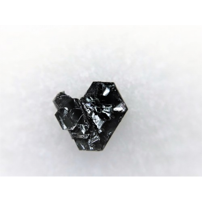
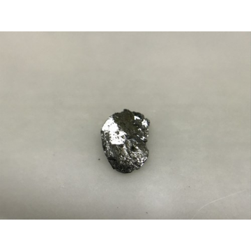
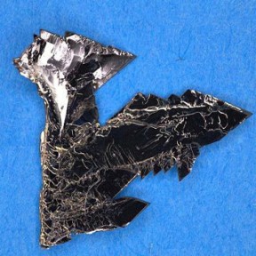
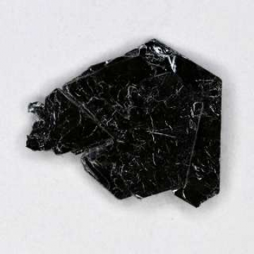
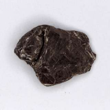
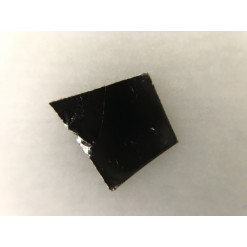
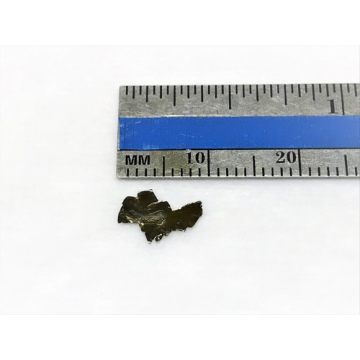
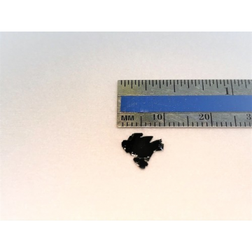
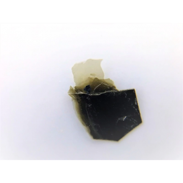
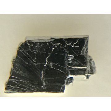
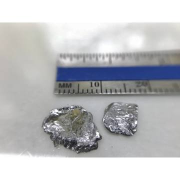
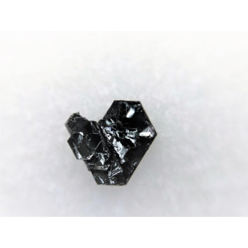
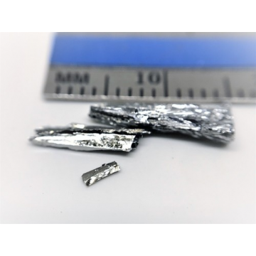
ZrSe2 belongs to group-IV TMDCs family and adopts a stable 2H-hexagonal structure. ZrSe2 is 0.95 eV indirect gap semiconductor in the bulk form. These ZrSe2 crystals were designed and optimized at our facilities starting 2013 to achieve perfect electronic grade materials with: 1) excellent stoichiometry, 2) large single domain size, 3) single phase materials without any mixed phases or amorphous content, 4) unmatched purity -electronic grade (6N), 99.9999% confirmed purity. Our crystals exhibit sharpest Raman and XRD peaks in the commercial market proving the high quality of our materials.
Properties of ZrSe2 layered crystals

Growth method matters> Flux zone or CVT growth method? Contamination of halides and point defects in layered crystals are well known cause for their reduced electronic mobility, reduced anisotropic response, poor e-h recombination, low-PL emission, and lower optical absorption. Flux zone technique is a halide free technique used for synthesizing truly semiconductor grade vdW crystals. This method distinguishes itself from chemical vapor transport (CVT) technique in the following regard: CVT is a quick (~2 weeks) growth method but exhibits poor crystalline quality and the defect concentration reaches to 1E11 to 1E12 cm-2 range. In contrast, flux method takes long (~3 months) growth time, but ensures slow crystallization for perfect atomic structuring, and impurity free crystal growth with defect concentration as low as 1E9 - 1E10 cm-2. During check out just state which type of growth process is preferred. Unless otherwise stated, 2Dsemiconductors ships Flux zone crystals as a default choice.
XRD data collected from ZrSe2 crystals

Raman spectrum collected from ZrSe2 layered crystals


宝贝与描述相符
5