-
关注商城

关注官方微信
关注官方微信

销售咨询
技术支持

联系客服


 购前提示 |
常用产品货期为1-2天,非常用产品为一周; 进口产品、贵金属产品、订制规格产品,价格、货期影响因素较多。 关于货期、价格、质量规格等问题采购前,请于客服沟通。 |
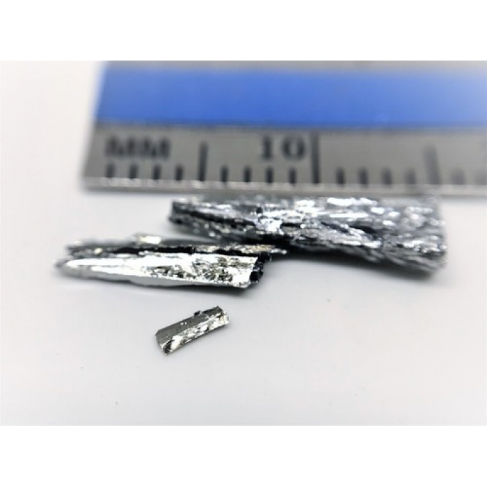
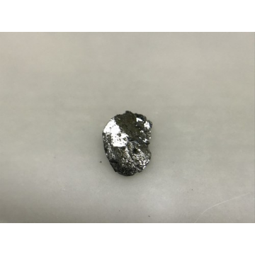
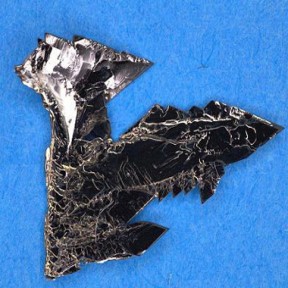
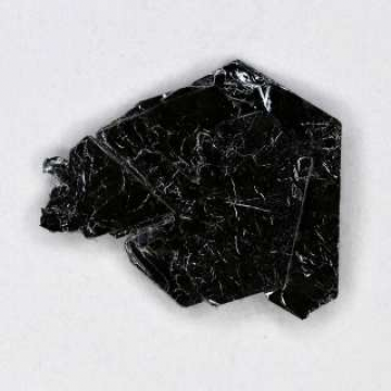
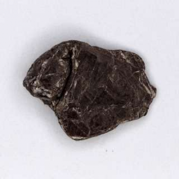
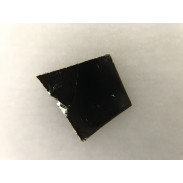
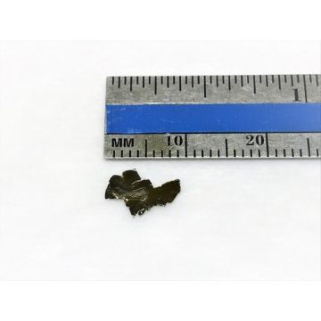
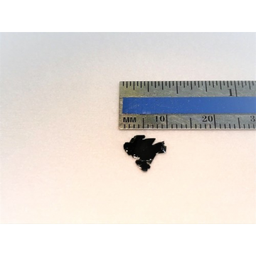
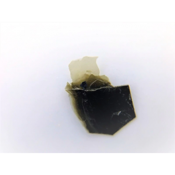
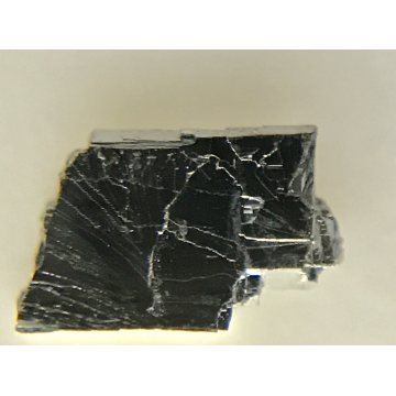
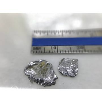
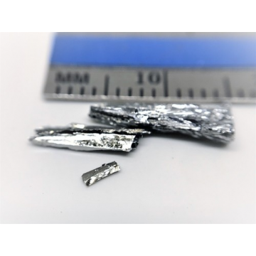
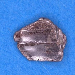
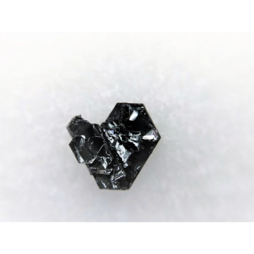
The first commercial vdW Tellurium (Bulk trigonal phase) crystals. Layered tellurium crystals have been synthesized in perfectly vdW order through flux zone growth technique. The crystal has 99.9999% (6N) rated purity and has been crystalized in perfect atomic order. Layered tellurium (Te) has a trigonal crystal lattice (see product images) in which individual helical chains of Te atoms are stacked together by van der Waals type bonds and spiral around axes parallel to the [0001] direction at the center and corners of the hexagonal elementary cell [1-2]. Tellurene exhibits a tunable bandgap varying from nearly direct 0.31 eV (bulk) to indirect 1.17 eV (2L) and direct at 1.3 eV (1L) [3]. It has four (two) complex, highly anisotropic and layer-dependent hole (electron) pockets in the first Brillouin zone with an extraordinarily high hole mobility reaching up to theoretical ∼1E5 cm2/Vs value [1-3].
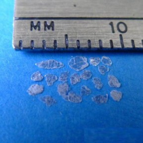
Physical size ~1cm or larger;
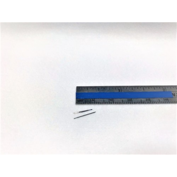
Monolayer Tellurene solutions are also available here
Raman spectrum collected from Tellurene crystals under 532 nm laser excitation

XRD data collected from tellurene crystals

Note: This product is same as tellurene material. While material itself is perfectly crystallized in trigonal form (weakly coupled Te chains are present), it is inherently harder to exfoliate in comparison to graphene or MoS2. For best results, we recommend using strongly adhesive tapes or liquid exfoliation technique.
Related references
[1] "Two-dimensional tellurium" Nature 552, 40-41 (2017) [Page link]
[2] "Large-area solution-grown 2D tellurene for air-stable, high-performance field-effect transistors"; arXiv:1704.06202 [Page link]
[3] "Few-layer Tellurium: one-dimensional-like layered elementary semiconductor with striking physical properties" ; https://doi.org/10.1016/j.scib.2018.01.010 [Page link]


宝贝与描述相符
5